A new wave for antennas

From solar panels to high-resolution imaging, a host of advanced technologies relies on the manipulation of light waves.
Engineers have traditionally bent light beams toward a desired focal point using glass lenses, according to Hossein Mosallaei, a professor of electrical and computer engineering at Northeastern University. But lenses are bulky and curved, limiting their ability to be incorporated onto the miniaturized, flat chips that enable today’s tiny devices.
When one thinks of antennas, on the other hand, the first thing that comes to mind is not usually light transmission. But the straight wires projecting from old-school mobile phones and the hood of grandpa’s Cadillac are just one type in a range of antenna technologies. As Mosallaei says, an antenna is merely something that can scatter an electromagnetic wave.
Giant dish antennas decorate vast desert expanses, sending and receiving microwaves from the distant reaches of the solar system. Even lenses, which reflect, transmit and bend light waves, are, technically speaking, antennas. Recently, Mosallaei has transformed the concept of array antennas, commonly used with microwave frequencies, to enable light engineering in the subwavelength scale.
Since the size of a metallic antenna is directly proportional to the wavelength of interest, very small wires are required for the very short wavelengths that make up the optical range. Mosallaei is leveraging that fact to design nanoscale antennas embedded in materials to tailor light in the optical frequency range.
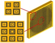
In 2011, Mosallaei’s research team released a paper in the journal Optics Letters, which ended up becoming the publication’s most downloaded article of the year. The paper laid out the first example of an array of tiny antennas arranged on a flat, thin-film substrate, called a metasurface. Each pixel of the substrate is dotted with a separate antenna, each of which receives an optical wave and locally bends it in a particular direction. “Now, if I shine light on it, magic happens,” said Mosallaei, who believes this new approach will create a new paradigm for optics engineering.
Of course, it’s not magic, but the precise tailoring of the wave’s amplitude and phase. With different antenna arrangements, Mosallaei’s metasurface can direct optical waves along any desired path. “This will be a transformative concept to make flat nanomaterials that can engineer the light in subwavelength scale,” said Mosallaei. Having inclusions of nanoantennas in a thin-film can feature unique optical characteristics, he said, such as engineered reflection, transmission, or absorption.
Additionally, since the nanoantennas are themselves smaller than the wavelengths they manipulate, they do a much better job of focusing light than lenses, which are limited by diffraction.
“If I can concentrate the light in an area of 20nm, instead of 400nm, this means interaction on smaller scales, leading to better sensing devices or higher-resolution imaging,” said Mosallaei. This feat can also help with new unconventional nanofabrication schemes.
Mosallaei’s team works on the theoretical and computational level, but in collaboration with George Whitesides, a professor of chemistry at Harvard University, prototypes of these metasurfaces are becoming a reality.
Read more here.
