Innovative Out-of-Plane Printed Design Boosts Electronics Efficiency and Performance

ECE Professor Ravinder Dahiya published “Out-of-Plane Electronics on Flexible Substrates Using Inorganic Nanowires Grown on High Aspect Ratio Printed Gold Micropillars” in Advanced Materials. The paper describes a new method of creating nanowire-based electronics that are more efficient in their manufacture and performance than current methods allow, potentially enabling more sensitive sensors or efficient energy harvesters.
Ravinder Dahiya, professor of electrical and computer engineering, has published research in Advanced Materials that details a new method of creating nanowire-based electronics that are more efficient in their manufacture and performance than current methods allow. The paper, “Out-of-Plane Electronics on Flexible Substrates Using Inorganic Nanowires Grown on High Aspect Ratio Printed Gold Micropillars,” describes a microscopic jet-printing technique to develop micropillars on which thick forests of nanowires are grown. These nanowires sit “out-of-plane” above a substrate. Multiplying the number of nanowires on the substrate in this way can increase the sensitivity of sensors or improve their capacity to capture light from wide angles to obtain efficient energy harvesters.
Dahiya and his team in the Bendable Electronics and Sustainable Technologies (BEST) group achieved this out-of-plane architecture using a microscopic nozzle to build up “micropillars” by spraying gold nanoparticles on a surface. These micropillars can reach up to 150 micrometers in height, much higher than traditional nanofabrication techniques can produce. Zinc-oxide nanowires were then grown on these micropillars, creating bushy structures that resemble narrow shrubs. The nanowires are light-sensitive, Dahiya explains—when light of a certain wavelength hits them, they change their electrical resistance. By arranging many of these shrub-like structures together on a substrate, one can create a volume of nanowires 15 to 20 times larger than what would be possible in a single layer on a flat surface.
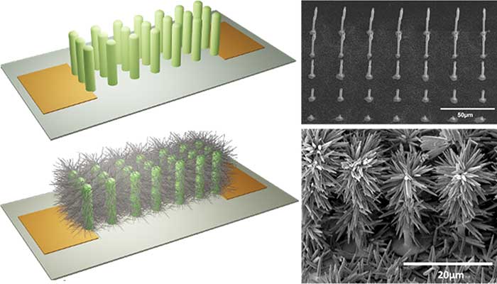
Schematic and microscope images of micropillars (top row), and micropillars with nanowires (bottom row)
“Growing nanowires on the pillar itself is quite a challenge,” Dahiya says, explaining that the gold used for the micropillars had to be combined with a binding agent to enable the printing process. “But by suitably tuning the printing parameters we were still able to get quite nice nanowires – in fact ones with the highest aspect ratio.”
Properties like light sensitivity can enable applications in photodetection electronics; in the case of zinc-oxide-based designs, perhaps a wearable sensor could be developed for healthcare to detect harmful ultraviolet radiation. Dahiya explains that nanowires made of other elements can have different optical or electrical properties, making them suitable for energy applications like solar cells, or thermal and optical surveillance systems.
Regardless of the application, this out-of-plane architecture increases efficiency in multiple ways. In terms of production, traditional lithography involves depositing metal on a surface and then etching it away—a subtractive method in which the material removed by etching is discarded. Printing, an additive means of fabrication, uses only as much material as needed and is inherently more resource-efficient and sustainable. In operation, out-of-plane designs can function more efficiently as well, as nanowires suspended above a substrate are exposed to more energy than those that lie flat on the surface. For applications like solar power, this would mean that cells could collect and use more sunlight with no increase in their surface area.
“If you’re reducing the resources you’re using to fabricate the device, and the device also gives you better outcomes, that really ticks both boxes,” Dahiya says.